PCB wiring is a key element of ESD protection. Reasonable PCB design can reduce unnecessary costs caused by fault inspection and rework. In PCB design, transient voltage suppressor (TVS) diodes are used to suppress direct charge injection caused by ESD discharge, so overcoming electromagnetic interference (EMI) effects caused by discharge current is more important in PCB design. This article will provide PCB design standards that can optimize ESD protection.
1. Loop Road
Current is induced into a closed circuit of magnetic flux changes. The amplitude of the current is proportional to the area of the loop. Larger circuits contain more magnetic flux, thus inducing stronger currents in the circuit. Therefore, it is necessary to reduce the circuit area.
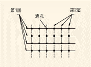
The most common loop is composed of power and ground. If possible, a multi-layer PCB design with power and ground layers can be adopted. Multilayer circuit boards not only minimize the loop area between power and ground, but also reduce the high-frequency EMI electromagnetic field generated by ESD pulses.

If multi-layer circuit boards cannot be used, the power and ground wires must be connected in a grid like pattern, as shown in Figure 2. Grid connection can serve as both a power source and a grounding layer. The printed circuit of each layer is connected through via holes, and the interval between via hole connections should be within 6cm in each direction. In addition, when wiring, the circuit area can also be reduced by placing the power and ground printed circuits as close as possible.
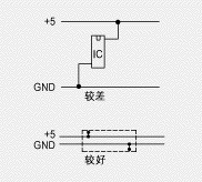
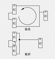
Another method to reduce the loop area and induced current is to reduce the parallel paths between interconnected devices, as shown in the figure.

When it is necessary to use signal connection wires with a length exceeding 30 centimeters, protective wires can be used, as shown in Figure 5. A better approach is to place a geological layer near the signal line. The signal line should be within 13mm of the protective or grounding wire layer.
Cross the long signal line (>30cm) or power line of each sensitive component with its grounding wire. Crosslines must be arranged at certain intervals from top to bottom or from left to right.
2. Circuit connection length
Long signal lines can also serve as antennas for receiving ESD pulse energy, and using shorter signal lines as much as possible can reduce the efficiency of signal lines as antennas for receiving ESD electromagnetic fields. Try to place interconnected devices adjacent to each other to reduce the length of interconnected printed circuits.
3. Ground charge injection

TVS diverts induced current and maintains the potential difference of TVS clamping voltage. TVS and capacitors should be placed as close as possible to the protected IC (see Figure 7), and the path from TVS to ground and the pin length of the capacitor should be minimized to reduce parasitic inductance effects.
The connector must be installed on the copper platinum layer on the PCB. Ideally, the Cu Pt layer must be isolated from the ground layer of the PCB and connected to the solder pads through short wires.
4. Other standards for PCB design
Avoid placing important signal lines such as clock and reset signals at the edge of the PCB;
Set the unused parts of the PCB as ground planes;
The distance between the grounding wire and the signal wire should be at least 4 millimeters;
Keep the aspect ratio of the chassis grounding less than 5:1 to reduce inductance effects;
TVS diodes are used to protect all external connections;
5. Protect parasitic inductance in the circuit
When an ESD event occurs, the parasitic inductance in the TVS diode path can cause severe voltage overshoot. Even with TVS diodes, excessive overshoot voltage may still exceed the damage voltage threshold of the protected IC due to the induced voltage VL=L × di/dt on the inductive load.
The total voltage that the protection circuit can withstand is the sum of the voltage clamped by the TVS diode and the voltage generated by parasitic inductance, VT=VC+VL。 The transient induced current of ESD can reach its peak in less than 1ns (according to IEC 61000-4-2 standard). Assuming the lead inductance is 20nH per inch and the line length is a quarter inch, the overshoot voltage is a pulse of 50V/10A. The rule of thumb is to design the shunt path as short as possible to reduce parasitic inductance effects.
All inductance paths must consider the path between the grounding circuit, TVS, and protected signal lines, as well as the path from the connector to the TVS equipment. The protected signal line should be directly connected to the ground plane. If there is no grounding layer, the connection of the grounding circuit should be as short as possible. The distance between the grounding of the TVS diode and the grounding point of the protected circuit should be as short as possible to reduce the parasitic inductance of the grounding layer.
Finally, TVS devices should be placed as close as possible to the connector to reduce transient coupling to nearby lines. Although there is no direct path to the connector, this secondary radiation effect can also cause disruptions in the operation of other parts of the circuit board.


